Driving Product Innovation in Semiconductor Industry

Nov 29, 2021
High-Tech | 11 min READ
    
Early adopters of PLM in the semiconductor industry achieved development cost reductions of up to 40% and improved methods to support product teams efficiently. In recent years, leading semiconductor companies have adopted a suite of more sophisticated processes, tools, and practices to cover the whole innovation process and get new products to the market faster and cheaper while delivering on growth targets. While the innovation graph has been impressive, for most companies, the tools & processes in place are insufficient to drive innovation with the new technology and increasing complexity of the semiconductor products of tomorrow. This blog traces the bottlenecks companies face while driving continuous technological innovations in their business processes and how effective PLM adoption can be the right fit to deal with the complexities…
Nitin Jindal
Nitin Jindal

Digital Partner

CMT Vertical

Birlasoft

 
The Need for Innovation in Semiconductor Industry
The semiconductor industry – the backbone of all modern-era digital devices and future technologies – has registered multi-fold growth in the past decade in terms of revenue generation. As these companies chart their future growth story, the 300mm silicon wafer market is expected to increase in 2021 by 5% in comparison to 2020. To support this demand, companies must keep up with their innovative streaks. Companies need to rethink how they can compete and create value in the future. While on the one hand, semiconductor companies have tools & processes in place to accomplish innovation, on the other hand, the chips are getting complex with tighter product introduction schedules and rigorous resource requirements. To win over these complexities, companies must possess established innovation processes, global manufacturing, design locations, Intellectual Property (IP) organic growth processes or licensing mechanisms, and the right equilibrium of technical capacity & capability to keep up with the latest technological trends.
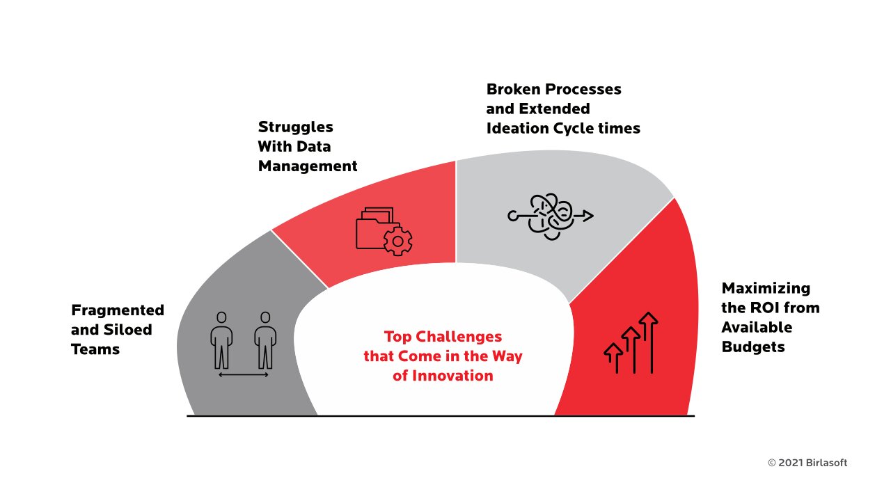
Top Challenges that Come in the Way of Innovation
Semiconductors – the unsung heroes of the technology world – are expanding their scope in next-generation smartphones, cars, medical equipment, etc. they are fast becoming a necessary technology for nearly every electronic device. If the recent innovations are anywhere to go by, semiconductor chips will need to rise beyond customers' expectations to capture a greater market share. With fierce competition in place, a logistical mishap, lax cost control, or misconstrued demand can severely impact a company's ROI. In tune with this, leading-edge chip design and manufacturing companies need to solve the maze obstructed by challenges enlisted below and start their journey towards continuous innovation.
Stay Ahead
Visit our High Tech page
 Putting Technology to Work
Fragmented and Siloed Teams
A semiconductor manufacturing capacity comprises complex nodes such as varied wafer sizes (100mm, 150mm, 200mm, 300mm, and the futuristic 450mm) and processes (from 350nm to 5nm), demanding a specific supply network. With such complex requirements to achieve, which requires them to deal with several internal & contractual manufacturing sites and distributions centers, no single semiconductor company can ever be self-sufficient. Additionally, they work with fragmented teams across the globe, requiring greater visibility and constant collaboration. If the semiconductor industry had continued on the yesteryear growth path, such fragmentations wouldn't have been challenging for companies. The moment new-age technologies started taking center stage, the need for innovation in the semiconductor value chain became evident.
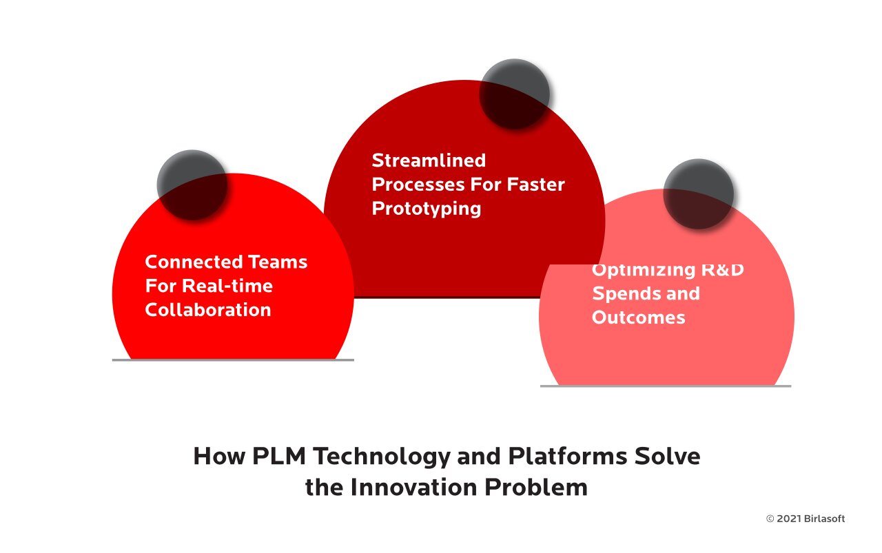
Such a complex web of the nonconnected network makes supply chain visibility difficult, leading to excess inventory growth and poor customer service. To simplify the productization, lessen engineering development cycle time and WIP (wafer-in-process) requirements for New Product Introduction (NPIs), companies need to expand their platform-based product design across families of products and generations, using the open sharing of technology roadmaps between customers and chip designers, again making a good case for PLM adoption in the semiconductor value chain.
Struggles With Data Management
Several research reports have confirmed that any strong advanced-analytics effort must start with the conception of a robust data set encompassing all necessary inputs – one that can be stored effectively and permits easy retrieval. This is a daunting task to achieve. In manufacturing, most leading-edge fabs have well-defined data models for individual tools. Each model requires sorting through 300 individual variables per tool or process steps. Some of these variables can be collected every few seconds or milliseconds, resulting in large volumes of data. In addition, inputs for each model may vary, depending on equipment or sensors in use or whether data is being analyzed while a process is underway or is completed.
Many companies find it challenging to align data sets or make comparisons. Overcoming these challenges warrants companies to go back to the original data and ensure aggregated consistently. Added to this are data latency issues arising out of data becoming stored in multiple disintegrated systems. In the absence of modern technology tools such as PLM, semiconductor companies find managing such a complex value chain challenging. This also calls for collaborative efforts to develop an interactive and agile supply chain that takes care of greater capacity, performance, and manufacturing costs.
Broken Processes and Extended Ideation Cycle times
According to a McKinsey study, on average, companies lose 33% of the PAT with the product shipment delay by six months compared to the losses of just 3.5% even if 50% is overspent in product development. The most successful semiconductor companies place a major thrust on first-pass success for new Integrated Circuit (IC) designs and product solutions. Low-quality first-pass designs also result in unacceptable yields, driving up cost, reducing profitability, and upending the final release and qualification requirements.
To give you a recent instance, one semiconductor company had to delay the launch of its flagship processor because of multiple design re-spins and low production yields, which resulted in angry customers and third-party developers and a huge dent in the company's market share. This example reflects that a successful first-pass design reduces market & development costs and amplifies new product revenue life. Design re-spins and software kit update massively enhance development costs and prolong the time-to-market for new products, frustrating customers.
Maximizing the ROI from Available Budgets
Attaining R&D leadership is not simply a tool for winning the market. It is also essential for controlling costs. For instance, the cost of building & equipping a facility with 5 nm production lines now runs about $5.4 billion—more than three times the $1.7 billion required for a fab with 10 nm production lines. Most of the cost increase is associated with the greater precision required to manufacture small structures. Additionally, as chip size gets smaller, R&D becomes more challenging because the researchers need to deal with quantum effects, minor structural variations, and factors that can complicate development. In the future, the R&D costs are only going to escalate, especially for leading-edge products.
While semiconductor companies need to dedicate billions of dollars to new fabs, they don't see an immediate RoI, which takes about 12 – 24 months to build a shell of a fab and install the required tools, with another 12 – 18 months for ramping up total capacity. Even after all these, if the demand falls beyond projections or if costs exceed expectations, the anticipated returns could be far lower than anticipated. While this is just one part of the problem, the semiconductor industry also needs to maintain a reliable track record for steady technological improvements to sustain its competitive edge. This calls for semiconductor companies to quickly find the right equilibrium between investment and R&D to garner sustainable RoI in the long run.
How PLM Technology and Platforms Solve the Innovation Problem
An efficient PLM captures data from different design, engineering, test, simulation, and validation platforms to create a complete picture of a product. This comprehensive, easy-to-find product data enables new streamlined processes. It focuses on ensuring that accurate, up-to-date data is readily available across disciplines, partners, and phases of a product's lifecycle. Another important tenet of PLM is a collaboration based on all needed information about engineering intent, decision criteria and rationale, and relevant events throughout the entire lifecycle.
 Putting Technology to Work
 Putting Technology to Work
Connected Teams For Real-time Collaboration
The innovation teams must share information and knowledge to achieve the product quality, reliability, performance, and cost to succeed. Fortunately, that is precisely what a PLM strategy does. Many semiconductor companies use PLM software to retool and support sharing, collaboration, understanding, and trust among experts to move toward the vision. It also enables those with less experience to make sound decisions because they have easy access to information that reflects the team's knowledge. Accelerating innovation in this fast-changing landscape requires a strong integration between mechanical, electrical, and software domains.
Traditional approaches do not permit these cross-domain collaborations, increasing the risk of quality issues, ensuing further costs and delays. An enhanced product development process captured in a digital thread not only offers better coordination of workflows and enhances collaboration across disciplines, but it can also automatically verify design proposals, virtually replacing the traditional design-build-test-break-redesign iteration process. This offers companies greater scope to explore more complex design optimization without incurring associated costs. It also ensures that those working on the process are using the latest information all the time.
Streamlined Processes For Faster Prototyping
PLM envisions systematic management of information throughout the entire lifecycle of the product in real-time. The information includes production and product design, product development and delivery process, performance management, and other phases of the product's lifecycle. The product lifecycle processes keep evolving in line with variables, such as functions, time, price, and performance. Given the constantly changing variables, a product innovation process adaptive enough to meet the new market requirements is paramount. PLM solutions help reduce operational costs and time to market. With the processes getting streamlined over time, prototyping becomes faster for semiconductor companies and thus quick time to market.
Optimizing R&D Spends and Outcomes
The ratio of the product lifecycle to product development time in semiconductors is half that for a mobile phone and a third that for an automobile, making a perfect case for R&D excellence the key differentiating factor. For successful semiconductor companies, managing their R&D investments and processes on a systematic and repeatable basis is of prudent importance, necessitating effective technology planning towards aligning R&D spending with current and future business strategies. This also requires harmonizing product and process innovations and leveraging a company's intellectual property to its fullest potential.
Intending to sustain and build up core competitiveness and further spur innovation, Shenzhen Hangsheng Electronics Co., Ltd. (Hangsheng Electronics) introduced digital design and production technologies to its R&D and manufacturing operations. The company optimized its overall PLM process to coordinate technical departments, manage design data, and schedule production, which helped share information across departments and utilize concurrent engineering throughout the design process.
To achieve this success, the company pursued a 'phased implementation' by dividing the PLM project into two phases – Propagating PLM best practices & knowledge, meeting the enterprise's applications requirements and effectively managing data; and integrating design & manufacturing, linking the whole R&D process via project management, dramatically upsurge the amount of data managed, etc. As part of this transformation exercise, the PLM system has been fully functional at its technical center and project management department and is also being deployed across manufacturing, quality control, product testing, and other departments. The whole product R&D process has brought profound benefits to the company during this journey.
Real-life Examples of PLM Tech-led Innovation in Chip Manufacturing
Today's PLM is an enterprise and ecosystem enabling platform for product innovation processes. As the name suggests, it spans processes across the lifecycle from concept through manufacturing. PLM also supports processes for more people and the entire product, not just one aspect. It integrates into other applications to pull data about suppliers, plus production operations at your sites and partners. In these ways, PLM supports more profitable innovation in many dimensions.
Example 1
A $2.5B fabless semiconductor company embraced PLM as a transformational initiative, choosing to implement PLM with a development product record. Like many companies, they were using in-house systems, such as a simple spreadsheet repository and a database client with a web interface. They could not efficiently collaborate with external suppliers, foundries, contractors, and manufacturing partners with no standardized tool or process to manage the product record.
To overcome the challenge, product data was transferred to new comprehensive PLM tools, which resulted in a robust enterprise solution. This enhanced solution captures all product groups and development teams and perfectly syncs with external suppliers, foundries, contractors, and manufacturing partners. PLM adoption has resulted in the company achieving a 15% reduction in development costs and a 50% cycle time reduction in validating change order requirements.
Example 2
SK Hynix started operating its M16 plant in early 2021 and is also planning to develop a semiconductor cluster in Yongin, South Korea, to strengthen the overall semiconductor ecosystem. The company-wide efforts demanded the efficient operation of these expanding production sites and the stabilization of the production system. As part of that, the DT organization successfully stabilized the M16 early this year and is now concentrating on advancing the production automation system in the long term.
The DT organization is currently establishing a PLM network to safeguard the integrity of the company-wide business process by integrating internal systems operating in siloes, which were impeding communication between teams. With the end-to-end visibility secured through PLM, decision-making and execution have become much more agile for the company.
In a world quickly transitioning towards a 'smart everything' scenario, the requirement of chips – from standard to highly customized, high precision, and high performance – is only slated to increase. The need to increase capacities and add new capabilities translates to massive capital expenditures, especially in semiconductor manufacturing. Semiconductor companies must leverage the latest technology tools to succeed in this new age of smart innovation and chart their growth journey through the rapidly changing business landscape.
With tools & processes built around the full innovation process, leading semiconductor companies are staying ahead in the market as judged by their product offerings and growth in the marketplace. By following their success stories, other companies need to quickly follow suit if they want to remain in the race to serve their customer; it seems to be the end of the road for them. The choice is YOURS!
 
 
Was this article helpful?